Spice Modelling And
Distortion Reduction
Analog Tape Recording
Kevin Aylward
kevin@kevinaylward.co.uk
Abstract
To
reduce the distortion of analog magnetic tape records, a larger higher
frequency, oscillator bias is added to the audio signal that is being recorded.
The reason for this is to minimize the distortion that is generated due to the
hysteresis of the magnetic material of the recording tape.
This
article provides a technique for the construction of standard spice models that
are able to model the essential characteristics of systems with this hysteresis.
The technique allows for an approximation of sufficiently accuracy to
illustrate hysteretic generated distortion and how it is reduced by the
addition of high frequency bias.
In
particular, the addition of a high frequency bias signal reduces distortion
because the large positive and negative magnetizations of the core due to the oscillator
bias signal, results in the audio signal magnetization being effectively a
linear average of the oscillator bias signal.
Key
words: high frequency bias, distortion, hysteresis, analog, tape recording,
spice, modelling
A Hysteresis Model
The
essential problem of modelling hysteresis is that it is a static or DC effect that
has memory. That is, the next value depends not only on the present value, but
also on the last value. However, this last value dependence does not depend on
time. This results in a multivalued transfer function. Unfortunately, standard
spice does not directly support this type of modelling. All dependence on the
last value in spice is usually the result of a linear integration, which
inherently results in frequency dependent transfer function and no account of
distortion mechanisms. A way around this
problem is to simply recognize that one can cheat. Analog models only have to do what they need to do, approximately, over a finite range
of frequencies. Analysis shows that a small capacitor in conjunction with nonlinear
diode resistances can be used to continuously store the last value of a signal
before it changes slope direction to provide an effective hysteresis, but
without unduly being dependent on frequency. This is in contrast to some spice “hysteresis”
models that are only two output state models that do not allow for a continuous
transfer function.
The Linear Model
The
following schematic forms the basis of a continuous hysteresis model that may
be used for modeling, for example, magnetic cores:

The
output voltage of this block, essentially, linearly follows the input, but with
an offset voltage. When the input turns around, the capacitor holds the voltage
such that there is a dead band starting from the peak voltage reached. The key
principle of operation is that there is nonlinear impedance that has a sharp
ratio of resistances for forward and reverse bias conditions. The standard
diode equation is the simplest, but not a necessary equation for the technique.
It is used here to illustrate the method. Alternative equations may be used to
fine tune the response characteristics. The input voltage may also be further
processed in order to achieve different nonlinear transfer curves. The example
here uses a behavioral model for the diodes of:
b1 a c
i={is}*(exp({k}*v(a,c)) - 1)
To
achieve an accurate model, the values of the components, are chosen such that
frequency effects are minimized, over the range of frequencies that the system
is desired to be modelled over. The time constant of Rload
and Cmemory should be such that the last voltage
before the turn around does not leak too much. The charging current through the
drive impedance (diodes in this particular case) is such to not limit the
response of the system over the desired operating frequency range.
The
above topology results in the following set of transfer functions, and
hysteresis graphs for various input voltages and frequencies:

Figure
1 – Ramped Input Transfer Function - F=1KHz,
VIN=2V, 4V, 6V, 8V, 10V

Figure 2 – Ramped Input Transfer Function - F=1MHz, VIN=2V, 4V, 6V, 8V, 10V
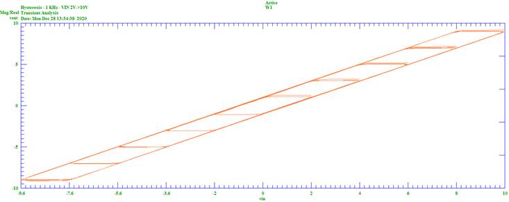
Figure 3 – Hysteresis - F=1kHz, VIN=2V, 4V, 6V, 8V, 10V

Figure 4 Hysteresis - F=1MHz, VIN=2V, 4V, 6V, 8V, 10V
The key points of the graphs, are that, over a 1000:1
frequency range, the voltage transfer function and the hysteresis voltage are
relatively constant, thus forming a good approximation to real DC hysteresis.
In general, one constructs a spice behavioural resistance
from a controlled current source that has the required forward and reverse
characteristics. For example, the hysteresis dead band voltage may be adjusted
by changing the diode parameter “N” from its default value of “1”.
Analog Tape
Distortion
The above model can now be used to analysis distortion
reduction in analog tape recorders when a high frequency sinewave bias signal
is added to the analog signal to be recorded.
To first order, consider that the tape does not enter
saturation such that this model does form a reasonable first order model to a
real core. That is, the dead band reflects the remanence of the core and that
this magnetic hysteresis results in a sinewave analog signal being clipped in a
manner to that shown in figures 1 & 2, with hysteresis shown in figures 3
& 4. Thus, it is evident that these hysteresis characteristics, causes
significant distortion.
Consider a large high frequency sinewave magnetization
signal. Even with hysteresis, the average of the recorded signal will be zero.
If this signal is now dc offset with another signal, the HF signals will now,
essentially, swing around this offset signal, independent of the dead band as
the large signal always drives the magnetization through the dead band. This is
true, despite the HF signal having waveform distortion. Thus, the average of
the HF bias signal will equal the offset signal, and it is this average value
that forms the recorded signal for playback. In this way, the offset signal
does not experience the dead band distortion as it would do if it was the only
applied signal. The wave shape of the HF bias does not matter so long as its
frequency is high enough such that all spurious signals are outside the bandwidth
of the desired signal, as they can be filtered out. A schematic illustrating
this is shown:

Figure 5 - Tape Distortion Reduction Schematic
The schematic shows the sum of 3 sinewave voltages.
Two signals represent a multi frequency input, with the other, the HF bias
signal. The two signals illustrate the effect of intermodulation distortion. A
nonlinear system will show sum and difference frequencies.
Typical, raw single input/output signals are shown
here:

Figure 6 - Single Frequency Signal, VIN=1V

Figure 7 - Single Frequency Signal, VIN=12V
Figure 6 & 7 shows the effective magnetization
signal “voltage lagging” it’s input, and subsequently
severely distorted due to the hysteresis that occurs when the signal changes
direction. A standard spice technique that generates a voltage lag would not
model this distortion of the waveform peaks.
The mixed, raw signal is shown here:
Figure
8 Mixed Frequency Signal, VINA=1V,
VINB=1V
Figure 8 shows that there is significant distortion of
the input signal.
FFTs of the mixed, unbiased signal are shown here:

Figure 9 - Unbiased Mixed Signal FFT VINA=1V, VINB=1V

Figure
10 Unbiased Mixed Signal FFT, VINA=6V, VINB=6V
These shows significant 500 Hz, 1kHz
and 1k5 intermodulation distortion for the unbiased condition
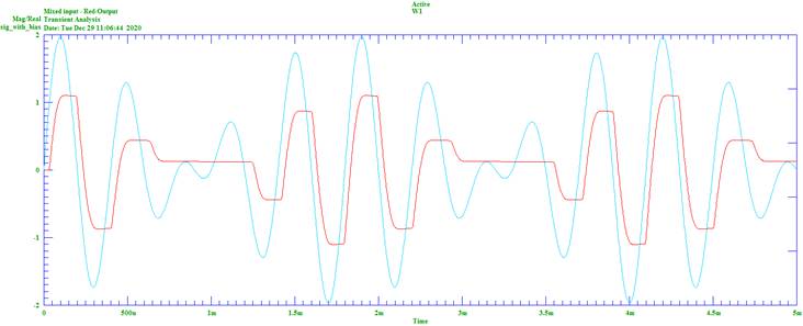
The mixed, HF biased signal is shown here:

Figure 11 - HF Biased, Mixed Signal
The FFT of the mixed, HF biased signal is shown here:

Figure 12 - HF Biased Mixed Signal FFT
The addition of the HF bias thus shows greatly reduced
intermodulation products.
Summary
This article has demonstrated a technique that allows
for the modelling of hysteresis within the capabilities of standard Spice. It
has also been shown how adding a high frequency bias signal to an audio signal
reduces distortion.