Analog Design
Kevin Aylward
B.Sc.
Delta-Sigma ADC
Alternative Linear Model
Back
to Contents
Overview
The purpose of this paper is to provide
an explanation and understanding as to the basic theory of Delta-Sigma A/D
converters. In particular, an alternative duty cycle linear/small signal model is
proposed that is mathematically and physically consistent, in contrast to the
standard linear model that is known to fail. It is not complete in the sense
that it is assumed that the reader has already read some of the conventional
literature on Sigma-Delta converters.
Essentially, all publications over the
last 30 years or so describing the basics of Delta-Sigma adc noise shaping
operation are incorrect.
By and large, these publications claim
that the large amplitude gain at low frequencies result in the reduction of
distortion of the 1 bit A/D in much the same manner as would be the case for
conventional slightly non-linear feedback system. For example, the article:
“Delta-Sigma Modulators: Tutorial Overview, Design
Guide, and State-of-the-Art Survey Circuits and Systems I:” IEEE Transactions
on (Volume:58 , Issue: 1 ) pub Dec. 2010
–
MathType@MTEF@5@5@+=feaagCart1ev2aqatCvAUfeBSjuyZL2yd9gzLbvyNv2CaerbuLwBLnhiov2DGi1BTfMBaeXatLxBI9gBaerbd9wDYLwzYbItLDharqqtubsr4rNCHbGeaGqiVu0Je9sqqrpepC0xbbL8F4rqqrFfpeea0xe9Lq=Jc9vqaqpepm0xbba9pwe9Q8fs0=yqaqpepae9pg0FirpepeKkFr0xfr=xfr=xb9adbaqaaeGaciGaaiaabeqaamaabaabaaGcbaacbaqcLbyaqaaaaaaaaaWdbiaa=nbiaaa@37C1@
J.M. de la Rosa
states:
“…Let
us consider that the gain of the loop filter is large inside the signal band
and small outside it. Due to the action of the feedback, the input signal, x,
and the analog version of the modulator output, y, will practically coincide
within the signal band. Consequently, most of the difference between both
signals will be placed at higher frequencies, i.e., the quantisation error, eq,
is shaped and most of its power is pushed outside the signal band…”
Technically, this statement is correct, however, the
statement is referring to signal amplitudes, and is strictly false based
on that assumption. The paper continues:
“Assuming that the quantiser in
Fig. 6 is represented by the linear additive white noise model…”
This assumption is false, and such an assumption
immediately leads to an incorrect physical conclusion.
Elementary feedback theory invalidates such a
linear model for such a grossly non-linear system. It is a trivial aspect of
analog amplifier theory that amplitude feedback can not reduce amplitude
distortion of a limiting amplifier. This is proven in this paper, and
illustrated in that such an assumption inherently results in noise shaping
equations that disagree with experiment. Principally, because some of the
comparator gain can theoretically and simply be moved to the integrator gain,
whence, this incorrect model then implies distortion is modifiable by changing
integrator gain, contrary to the known facts.
Additional facets of this, essentially, incorrect
understanding of Delta-Sigma operation has, apparently, led to misunderstanding
by some, of a fundamental error property of the Delta-Sigma converter that is a
trivial consequence of acknowledging that the Delta-Sigma converter is a
duty cycle modulator. This is the, apparently, previously unexplained (ref 4),
property that noise tones with a frequency proportional to the average dc input
up to mid scale, then folded, are produced. That is, this is what a Delta-Sigma
ADC does by inherent design!
Introduction
Conventional descriptions of Delta-Sigma
converters typically begin with a simplified block diagram of the physical
schematic of a 1 Bit A/D Delta-Sigma converter. A particular linear model is
then proposed with which it is alleged to mathematically show that quantisation
“noise” is reduced by action of frequency gain processing in a feedback loop.
The loop in this model is, essentially, based on instantaneous signal amplitudes
such as voltage and current, although performed in the Laplace S, or discrete
time Z domains.
A basic problem with this approach is
that the only rational interpretation of a reasonable formulation for such a
model is that the model predicts that the noise should be reducible to zero,
for all frequencies, despite the universal consensuses in the community is that
the model correctly predicts “noise shaping” with a result that apparently agrees
with the detailed non-linear time simulations and physical results. In order to
achieve this result the universal consensus also unilaterally agree to set an
inherent integrator gain constant parameter of the model to unity, despite
there being no mathematical or physical basis to make such an assumption, and
that detailed simulations show that the noise is independent of such gain
constant, even by several orders of magnitude change. What is perhaps even more
note worthy is that this basic anomalous result of the integrator gain constant
is also fully known in the community, yet the notion that this anomaly actually
means that the purported explanation of noise filtering by the feedback loop is
therefore false, appears to go unnoticed. Many papers reiterate that the
linear model, as proposed, explains noise filtering when clearly, cherry
picking the one specific value of a parameter so that it fits a desired result is
no explanation at all, and that an alternative approach is required. Indeed,
accepting such an explanation may be said to be on a par of using the Phlogiston
theory of fire to explain a one off occurrence of burning.
It is shown here that the root cause of
the failure of the standard linear model is due to the following:
1 Failure to recognise the basic incorrectness
of applying linear voltage/current theory to a 1 Bit A/D converter.
2 Failure to recognise that the Delta-Sigma
converter is not an over-sampled PCM converter but, essentially, it is inherently
a (variable discrete ) duty cycle modulator (strictly, a pulse density
modulator). That is, the Delta-Sigma converter achieves its accuracy by converting
signals in the amplitude (voltage/current) domain to the time domain.
Measurements in the time domain are then converted back to the amplitude
domain.
The distinction between PCM and (effective) PWM has
a drastic effect on anticipated distortion. This can be ascertained from
comparing to the non quantised equivalents, linear PAM (pulse amplitude
modulation) and linear PWM. For the PAM signal, only frequencies at NFs
+/- Fm are produced. For PWM a spectrum of NFs +/- MFm
are produced.
Standard Delta-Sigma Physical Model
A standard block diagram of the Delta Sigma
operation blocks is shown:
Fig. 1
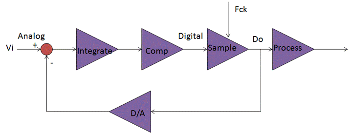
The basic operation being described as:
The difference between the input voltage
and output voltage is integrated in a direction such that if the input is not
equal to the digital output, converted to analog, the digital output will,
after time, be switched to an output value that will attempt it to equal the
input. The net result is that the average of the digital switching output
will be forced to equal the average input scaled by the DAC reference voltage.
The average of the digital output is
given by the ratio of the number digital highs to the sum of high and lows.
These numbers are determined by counts in time, determined by a reference
clock, and so the average may have a resolution determined by as many counts
are counted. Thus, the Sigma-Delta converter converts an input voltage to time,
and this time is then converted to a digital representation of the inputs amplitude.
Specifically, the integrator capacitor cannot pass
a steady state DC current, as it is an open circuit for DC. That is, a
capacitor’s average current must be exactly zero. This is so, even if
the capacitor is non-linear. For a typical converter with a common summing junction
for the input and feedback signals, this means that the average of the feedback
current minus the input current must be zero.
It is noted that the distinction between
a standard multibit PCM is that a for PCM a single sample represents,
essentially, a valid representation of the input signal. For a Delta-Sigma
converter, a single sample represents, essentially, nothing. Only multiple samples, have any meaning in
such a converter. This distinction is of fundamental importance when attempting
to form a linearised model of the Delta-Sigma converter.
Nominal Characteristics
The acknowledgment that the Delta-Sigma
converter is fundamentally and inherently a (variable) duty cycle based
converter, and not a PCM converter, allows a number of points to be made.
The actual average duty cycle does not usually
dictate a unique switching frequency. However, any repetitive average duty
cycle due to a constant DC voltage well result in a “noise” or idle tone frequency
component. That is:
τ
T
=
V
i
V
r
MathType@MTEF@5@5@+=feaagCart1ev2aqatCvAUfeBSjuyZL2yd9gzLbvyNv2CaerbuLwBLnhiov2DGi1BTfMBaeXatLxBI9gBaerbd9wDYLwzYbItLDharqqtubsr4rNCHbGeaGqiVv0Je9sqqrpepC0xbbL8F4rqaqFfpeea0xe9Lq=Jc9vqaqpepm0xbba9pwe9Q8fs0=yqaqpepae9pg0FirpepeKkFr0xfr=xfr=xb9adbaqaaeGaciGaaiaabeqaamaabaabaaGcbaWaaSaaaeaacqaHepaDaeaacaWGubaaaiabg2da9maalaaabaGaamOvamaaBaaaleaacaWGPbaabeaaaOqaaiaadAfadaWgaaWcbaGaamOCaaqabaaaaaaa@3DA6@
For a system nominally referenced to a 0V
to Vref DAC output voltage.
The period T, and hence the idle tones,
may well change with time as the system hunts to obtain a duty cycle that
equals the relative input voltage, however the minimum frequency is dictated by
the sampling frequency in that
τ
MathType@MTEF@5@5@+=feaagCart1ev2aqatCvAUfeBSjuyZL2yd9gzLbvyNv2CaerbuLwBLnhiov2DGi1BTfMBaeXatLxBI9gBaerbd9wDYLwzYbItLDharqqtubsr4rNCHbGeaGqiVv0Je9sqqrpepC0xbbL8F4rqaqFfpeea0xe9Lq=Jc9vqaqpepm0xbba9pwe9Q8fs0=yqaqpepae9pg0FirpepeKkFr0xfr=xfr=xb9adbaqaaeGaciGaaiaabeqaamaabaabaaGcbaGaeqiXdqhaaa@37AA@
can not be less than the sampling period. Therefore,
a Delta-Sigma converter may well have at least one error frequency no higher
than:
F
min
=
V
i
V
r
F
s
MathType@MTEF@5@5@+=feaagCart1ev2aqatCvAUfeBSjuyZL2yd9gzLbvyNv2CaerbuLwBLnhiov2DGi1BTfMBaeXatLxBI9gBaerbd9wDYLwzYbItLDharqqtubsr4rNCHbGeaGqiVv0Je9sqqrpepC0xbbL8F4rqaqFfpeea0xe9Lq=Jc9vqaqpepm0xbba9pwe9Q8fs0=yqaqpepae9pg0FirpepeKkFr0xfr=xfr=xb9adbaqaaeGaciGaaiaabeqaamaabaabaaGcbaGaamOramaaBaaaleaaciGGTbGaaiyAaiaac6gaaeqaaOGaeyypa0ZaaSaaaeaacaWGwbWaaSbaaSqaaiaadMgaaeqaaaGcbaGaamOvamaaBaaaleaacaWGYbaabeaaaaGccaWGgbWaaSbaaSqaaiaadohaaeqaaaaa@40C4@
This minimum frequency duty cycle will
set a limit to the minimum dc quantisable signal at Fs for a 1 bit converter as
follows.
The output can only switch from n 0s to
one 1 pulse at an on time of 1/Fs.
The minimum duty cycle possible is
therefore
D
min
=
τ
o
n
τ
o
MathType@MTEF@5@5@+=feaagCart1ev2aqatCvAUfeBSjuyZL2yd9gzLbvyNv2CaerbuLwBLnhiov2DGi1BTfMBaeXatLxBI9gBaerbd9wDYLwzYbItLDharqqtubsr4rNCHbGeaGqiVv0Je9sqqrpepC0xbbL8F4rqaqFfpeea0xe9Lq=Jc9vqaqpepm0xbba9pwe9Q8fs0=yqaqpepae9pg0FirpepeKkFr0xfr=xfr=xb9adbaqaaeGaciGaaiaabeqaamaabaabaaGcbaGaamiramaaBaaaleaaciGGTbGaaiyAaiaac6gaaeqaaOGaeyypa0ZaaSaaaeaacqaHepaDdaWgaaWcbaGaam4BaaqabaaakeaacaWGUbGaeqiXdq3aaSbaaSqaaiaad+gaaeqaaaaaaaa@4193@
This represents an output frequency of
F
o_min
=
1
n
τ
o
=
F
s
n
MathType@MTEF@5@5@+=feaagCart1ev2aqatCvAUfeBSjuyZL2yd9gzLbvyNv2CaerbuLwBLnhiov2DGi1BTfMBaeXatLxBI9gBaerbd9wDYLwzYbItLDharqqtubsr4rNCHbGeaGqiVv0Je9sqqrpepC0xbbL8F4rqaqFfpeea0xe9Lq=Jc9vqaqpepm0xbba9pwe9Q8fs0=yqaqpepae9pg0FirpepeKkFr0xfr=xfr=xb9adbaqaaeGaciGaaiaabeqaamaabaabaaGcbaGaamOramaaBaaaleaacaWGVbGaai4xaiGac2gacaGGPbGaaiOBaaqabaGccqGH9aqpdaWcaaqaaiaaigdaaeaacaWGUbGaeqiXdq3aaSbaaSqaaiaad+gaaeqaaaaakiabg2da9maalaaabaGaamOramaaBaaaleaacaWGZbaabeaaaOqaaiaad6gaaaaaaa@4544@
and an average dc output voltage of
V
min
=
V
ref
n
MathType@MTEF@5@5@+=feaagCart1ev2aqatCvAUfeBSjuyZL2yd9gzLbvyNv2CaerbuLwBLnhiov2DGi1BTfMBaeXatLxBI9gBaerbd9wDYLwzYbItLDharqqtubsr4rNCHbGeaGqiVv0Je9sqqrpepC0xbbL8F4rqaqFfpeea0xe9Lq=Jc9vqaqpepm0xbba9pwe9Q8fs0=yqaqpepae9pg0FirpepeKkFr0xfr=xfr=xb9adbaqaaeGaciGaaiaabeqaamaabaabaaGcbaGaamOvamaaBaaaleaaciGGTbGaaiyAaiaac6gaaeqaaOGaeyypa0ZaaSaaaeaacaWGwbWaaSbaaSqaaiaadkhacaWGLbGaamOzaaqabaaakeaacaWGUbaaaaaa@3FAE@
.
This is an inherent lower limit for
determining a Vmin input, as is not possible to achieve a smaller
duty cycle than that which is dictated by n.
To enable this frequency to be filtered
out, the input frequency must therefore satisfy:
F
s
>
V
i
V
ref
F
i
=n
F
i
MathType@MTEF@5@5@+=feaagCart1ev2aqatCvAUfeBSjuyZL2yd9gzLbvyNv2CaerbuLwBLnhiov2DGi1BTfMBaeXatLxBI9gBaerbd9wDYLwzYbItLDharqqtubsr4rNCHbGeaGqiVv0Je9sqqrpepC0xbbL8F4rqaqFfpeea0xe9Lq=Jc9vqaqpepm0xbba9pwe9Q8fs0=yqaqpepae9pg0FirpepeKkFr0xfr=xfr=xb9adbaqaaeGaciGaaiaabeqaamaabaabaaGcbaGaamOramaaBaaaleaacaWGZbaabeaakiabg6da+maalaaabaGaamOvamaaBaaaleaacaWGPbaabeaaaOqaaiaadAfadaWgaaWcbaGaamOCaiaadwgacaWGMbaabeaaaaGccaWGgbWaaSbaaSqaaiaadMgaaeqaaOGaeyypa0JaamOBaiaadAeadaWgaaWcbaGaamyAaaqabaaaaa@449F@
That is, if n is made larger to achieve
a lower coded input voltage, then the input frequency must be reduced so that
the minimum frequency duty cycle frequency can be filtered out.
Note that the argument is flipped when
considering the maximum duty cycle. In this case n represents voltages
reducing away from the maximum, which reduces the frequency.
Essentially, predictions for Fmin > Fs/2 are folded down to a
lower frequency about Fs/2.
This means that to achieve a true
resolution of 1/n, the signal must be over sampled by n in a 1 bit Delta Sigma
converter. This is so, irrespective of the order of the modulator, despite
contrary statements in the literature, although this has been recognised in the
literature (ref 12). Any attempt to produce the exact same average duty
cycle can only result in lower frequency components as it is not possible to have
smaller on or off times than that dictated by the clock period.
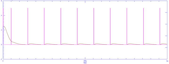
This has been verified in simulations. A
typical semi ideal simulation in the SuperSpice simulator
produced the following waveforms for a full scale of 0V to 5V set to nominally
1/100, or 50mv, of full scale DC input with a clock of 1Mhz, The output frequency was measured at 10.05kHz,
with the average digital output measured at 50.00mV. Also confirmed were
inverted waveforms for 50mV away from full saclae i.e 4.95V for these
simulations.
Fig. 2
100th full scale Delta-Sigma
digital output and 16 kHz filtered DC voltage output
It may be noted, that in general, mid
range voltages typically allow for the duty cycle to oscillate, pseudo
randomly, such that the duty cycle may go high and low but still achieve a net
average 0 and 1’s density that corresponds to an exact Vin/Vref
but which has no fundamental steady state oscillation error noise frequency. However,
any rational value of Vin/Vref will result in an exact
solution to the ideal feedback property of the system that
τ
MathType@MTEF@5@5@+=feaagCart1ev2aqatCvAUfeBSjuyZL2yd9gzLbvyNv2CaerbuLwBLnhiov2DGi1BTfMBaeXatLxBI9gBaerbd9wDYLwzYbItLDharqqtubsr4rNCHbGeaGqiVv0Je9sqqrpepC0xbbL8F4rqaqFfpeea0xe9Lq=Jc9vqaqpepm0xbba9pwe9Q8fs0=yqaqpepae9pg0FirpepeKkFr0xfr=xfr=xb9adbaqaaeGaciGaaiaabeqaamaabaabaaGcbaGaeqiXdqhaaa@37AA@
/T = Vin/Vref, therefore
at such rational values, tones should be generated.
Standard Delta-Sigma Linear Noise
Model
A standard block diagram of the Delta Sigma
linear noise model is shown:
Fig. 3

The physical 1 Bit A/D (comparator) has
been replaced by a unity gain summer with an added error source representing
the error between the A/D output and its analog input. The input and output
voltages have been replaced by a Z domain representation of the instantaneous
signal amplitudes. However, although it is often noted that such a gross
linearisation approximation to the A/D has some issues, its true nature that
such a model is, essentially, useless, is usually ignored. Possibly because the
end justifies the means!
It is now shown that such a model in a transfer
function feedback loop is fundamentally invalid, and that such a model
inherently results in a model with predictions that disagree with reality.
Invalidity Of The 1 Bit A/D Noise Model
Consider an amplifier driving a 1 bit A/D
converter. It is shown here that such a system is so grossly non linear that
voltage/current transfer feedback can not reduce the distortion as would be the
case for relatively weakly non linear systems. This is actually, intuitively
obvious, for clearly if the output of a block can only be one of two values by
design, nothing can be done to change those values. It is however instructive
to formally show this by general feedback theory, as for example in the paper Feedback Distortion, from which a
key argument is repeated here, and should be read to gain an understanding as
to when feedback is able to reduce distortion..
Fig. 4

Vo is either Vr or
–
MathType@MTEF@5@5@+=feaagCart1ev2aqatCvAUfeBSjuyZL2yd9gzLbvyNv2CaerbuLwBLnhiov2DGi1BTfMBaeXatLxBI9gBaerbd9wDYLwzYbItLDharqqtubsr4rNCHbGeaGqiVu0Je9sqqrpepC0xbbL8F4rqqrFfpeea0xe9Lq=Jc9vqaqpepm0xbba9pwe9Q8fs0=yqaqpepae9pg0FirpepeKkFr0xfr=xfr=xb9adbaqaaeGaciGaaiaabeqaamaabaabaaGcbaacbaqcLbyaqaaaaaaaaaWdbiaa=nbiaaa@37C1@
Vr depending on whether A.Vd
is greater or less than zero.
It is sometimes proposed to model such a
system by the following:
Fig. 5

For the non feedback case, an expression
for the output Vo is assumed to be of the form:
V
o
=S+D
MathType@MTEF@5@5@+=feaagCart1ev2aqatCvAUfeBSjuyZL2yd9gzLbvyNv2CaerbuLwBLnhiov2DGi1BTfMBaeXatLxBI9gBaerbd9wDYLwzYbItLDharqqtubsr4rNCHbGeaGqiVDI8FfYJH8YrFfeuY=Hhbbf9v8qqaqFr0xc9pk0xbba9q8WqFfeaY=biLkVcLq=JHqpepeea0=as0Fb9pgeaYRXxe9vr0=vr0=vqpWqaaeaabiGaciaacaqabeaadaqaaqaaaOqaaiaadAfadaWgaaWcbaGaam4BaaqabaGccqGH9aqpcaWGtbGaey4kaSIaamiraaaa@3BB8@
That is, the wanted signal, S,
plus an error term D.
In which case, the relations for S and D
would be, for Vi > 0+:
S=A
V
i
MathType@MTEF@5@5@+=feaagCart1ev2aqatCvAUfeBSjuyZL2yd9gzLbvyNv2CaerbuLwBLnhiov2DGi1BTfMBaeXatLxBI9gBaerbd9wDYLwzYbItLDharqqtubsr4rNCHbGeaGqiVDI8FfYJH8YrFfeuY=Hhbbf9v8qqaqFr0xc9pk0xbba9q8WqFfeaY=biLkVcLq=JHqpepeea0=as0Fb9pgeaYRXxe9vr0=vr0=vqpWqaaeaabiGaciaacaqabeaadaqaaqaaaOqaaiaadofacqGH9aqpcaWGbbGaamOvamaaBaaaleaacaWGPbaabeaaaaa@3AC3@
D=(1−
A
V
i
V
r
)
V
r
MathType@MTEF@5@5@+=feaagCart1ev2aqatCvAUfeBSjuyZL2yd9gzLbvyNv2CaerbuLwBLnhiov2DGi1BTfMBaeXatLxBI9gBaerbd9wDYLwzYbItLDharqqtubsr4rNCHbGeaGqiVDI8FfYJH8YrFfeuY=Hhbbf9v8qqaqFr0xc9pk0xbba9q8WqFfeaY=biLkVcLq=JHqpepeea0=as0Fb9pgeaYRXxe9vr0=vr0=vqpWqaaeaabiGaciaacaqabeaadaqaaqaaaOqaceaa4JIaamiraiabg2da9iaacIcacaaIXaGaeyOeI0YaaSaaaeaacaWGbbGaamOvamaaBaaaleaacaWGPbaabeaaaOqaaiaadAfadaWgaaWcbaGaamOCaaqabaaaaOGaaiykaiaadAfadaWgaaWcbaGaamOCaaqabaaaaa@42F8@
V
o
=A
V
i
+(1−
A
V
i
V
r
)
V
r
MathType@MTEF@5@5@+=feaagCart1ev2aqatCvAUfeBSjuyZL2yd9gzLbvyNv2CaerbuLwBLnhiov2DGi1BTfMBaeXatLxBI9gBaerbd9wDYLwzYbItLDharqqtubsr4rNCHbGeaGqiVDI8FfYJH8YrFfeuY=Hhbbf9v8qqaqFr0xc9pk0xbba9q8WqFfeaY=biLkVcLq=JHqpepeea0=as0Fb9pgeaYRXxe9vr0=vr0=vqpWqaaeaabiGaciaacaqabeaadaqaaqaaaOqaaiaadAfadaWgaaWcbaGaam4BaaqabaGccqGH9aqpcaWGbbGaamOvamaaBaaaleaacaWGPbaabeaakiabgUcaRiaacIcacaaIXaGaeyOeI0YaaSaaaeaacaWGbbGaamOvamaaBaaaleaacaWGPbaabeaaaOqaaiaadAfadaWgaaWcbaGaamOCaaqabaaaaOGaaiykaiaadAfadaWgaaWcbaGaamOCaaqabaaaaa@46B8@
Because for any value Vi greater
than zero, the output, Vo, is the constant Vr. A similar
expression may be written for the case is less than zero. Applying feedback by
letting Vi -> Vi - Vo:
V
o
=A(
V
i
−
V
o
)+(1−
A(
V
i
−
V
o
)
V
r
)
V
r
MathType@MTEF@5@5@+=feaagCart1ev2aaatCvAUfeBSjuyZL2yd9gzLbvyNv2CaerbuLwBLnhiov2DGi1BTfMBaeXatLxBI9gBaerbd9wDYLwzYbItLDharqqtubsr4rNCHbGeaGqiVDI8FfYJH8YrFfeuY=Hhbbf9v8qqaqFr0xc9pk0xbba9q8WqFfeaY=biLkVcLq=JHqpepeea0=as0Fb9pgeaYRXxe9vr0=vr0=vqpWqaaeaabiGaciaacaqabeaadaqaaqaaaOqaaiaadAfadaWgaaWcbaGaam4BaaqabaGccqGH9aqpcaWGbbGaaiikaiaadAfadaWgaaWcbaGaamyAaaqabaGccqGHsislcaWGwbWaaSbaaSqaaiaad+gaaeqaaOGaaiykaiabgUcaRiaacIcacaaIXaGaeyOeI0YaaSaaaeaacaWGbbGaaiikaiaadAfadaWgaaWcbaGaamyAaaqabaGccqGHsislcaWGwbWaaSbaaSqaaiaad+gaaeqaaOGaaiykaaqaaiaadAfadaWgaaWcbaGaamOCaaqabaaaaOGaaiykaiaadAfadaWgaaWcbaGaamOCaaqabaaaaa@4F4D@
V
o
(1+A−A)=A
V
i
+(1−
A
V
i
V
r
)
V
r
MathType@MTEF@5@5@+=feaagCart1ev2aaatCvAUfeBSjuyZL2yd9gzLbvyNv2CaerbuLwBLnhiov2DGi1BTfMBaeXatLxBI9gBaerbd9wDYLwzYbItLDharqqtubsr4rNCHbGeaGqiVDI8FfYJH8YrFfeuY=Hhbbf9v8qqaqFr0xc9pk0xbba9q8WqFfeaY=biLkVcLq=JHqpepeea0=as0Fb9pgeaYRXxe9vr0=vr0=vqpWqaaeaabiGaciaacaqabeaadaqaaqaaaOqaaiaadAfadaWgaaWcbaGaam4BaaqabaGccaGGOaGaaGymaiabgUcaRiaadgeacqGHsislcaWGbbGaaiykaiabg2da9iaadgeacaWGwbWaaSbaaSqaaiaadMgaaeqaaOGaey4kaSIaaiikaiaaigdacqGHsisldaWcaaqaaiaadgeacaWGwbWaaSbaaSqaaiaadMgaaeqaaaGcbaGaamOvamaaBaaaleaacaWGYbaabeaaaaGccaGGPaGaamOvamaaBaaaleaacaWGYbaabeaaaaa@4C26@
V
o
=A
V
i
+(1−
A
V
i
V
r
)
V
r
MathType@MTEF@5@5@+=feaagCart1ev2aaatCvAUfeBSjuyZL2yd9gzLbvyNv2CaerbuLwBLnhiov2DGi1BTfMBaeXatLxBI9gBaerbd9wDYLwzYbItLDharqqtubsr4rNCHbGeaGqiVDI8FfYJH8YrFfeuY=Hhbbf9v8qqaqFr0xc9pk0xbba9q8WqFfeaY=biLkVcLq=JHqpepeea0=as0Fb9pgeaYRXxe9vr0=vr0=vqpWqaaeaabiGaciaacaqabeaadaqaaqaaaOqaaiaadAfadaWgaaWcbaGaam4BaaqabaGccqGH9aqpcaWGbbGaamOvamaaBaaaleaacaWGPbaabeaakiabgUcaRiaacIcacaaIXaGaeyOeI0YaaSaaaeaacaWGbbGaamOvamaaBaaaleaacaWGPbaabeaaaOqaaiaadAfadaWgaaWcbaGaamOCaaqabaaaaOGaaiykaiaadAfadaWgaaWcbaGaamOCaaqabaaaaa@46B7@
This expression is, as expected, clearly,
the same as the original expression, therefore, for a 1 Bit A/D, voltage/current
transfer function, feedback can do nothing to the inherent signal to distortion/error
ratio. That is, standard linear feedback loop analysis for the 1 bit A/D
converter, for essentially instantaneous voltage/current signals is completely
invalid.
Standard Delta-Sigma
Noise Analysis
A standard block diagram of Delta Sigma
linear noise analysis is shown:
Fig. 6
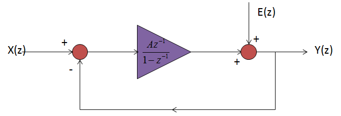
In standard treatments, the gain factor
A is omitted, however there is no mathematical or physical justification for
this omission. The main block represents the Delta Sigma integrator. This integrator feeds an A/D converter, that
is, a comparator, which is ideally, an infinite gain amplifier. Some of the
gain of the comparator can logically, simply be assigned to the integrator as
the integrator and comparator are in series cascade. The analysis of the loop then
results in:
Y(z)=
X(z)A
z
−1
1+(A−1)
z
−1
+
E(z)(1−
z
−1
)
1+(A−1)
z
−1
MathType@MTEF@5@5@+=feaagCart1ev2aaatCvAUfeBSjuyZL2yd9gzLbvyNv2CaerbuLwBLnhiov2DGi1BTfMBaeXatLxBI9gBaerbd9wDYLwzYbItLDharqqtubsr4rNCHbGeaGqiVDI8FfYJH8YrFfeuY=Hhbbf9v8qqaqFr0xc9pk0xbba9q8WqFfeaY=biLkVcLq=JHqpepeea0=as0Fb9pgeaYRXxe9vr0=vr0=vqpWqaaeaabiGaciaacaqabeaadaqaaqaaaOqaaiaadMfacaGGOaGaamOEaiaacMcacqGH9aqpdaWcaaqaaiaadIfacaGGOaGaamOEaiaacMcacaWGbbGaamOEamaaCaaaleqabaGaeyOeI0IaaGymaaaaaOqaaiaaigdacqGHRaWkcaGGOaGaamyqaiabgkHiTiaaigdacaGGPaGaamOEamaaCaaaleqabaGaeyOeI0IaaGymaaaaaaGccqGHRaWkdaWcaaqaaiaadweacaGGOaGaamOEaiaacMcacaGGOaGaaGymaiabgkHiTiaadQhadaahaaWcbeqaaiabgkHiTiaaigdaaaGccaGGPaaabaGaaGymaiabgUcaRiaacIcacaWGbbGaeyOeI0IaaGymaiaacMcacaWG6bWaaWbaaSqabeaacqGHsislcaaIXaaaaaaaaaa@5BBB@
Where X(Z), Y(Z) are the Z transform of
the instantaneous time domain amplitudes (voltages) x(KT), y(KT)
The standard treatment with A=1 simply
gives:
Y(z)=X(z)
z
−1
+E(z)(1−
z
−1
)
MathType@MTEF@5@5@+=feaagCart1ev2aaatCvAUfeBSjuyZL2yd9gzLbvyNv2CaerbuLwBLnhiov2DGi1BTfMBaeXatLxBI9gBaerbd9wDYLwzYbItLDharqqtubsr4rNCHbGeaGqiVDI8FfYJH8YrFfeuY=Hhbbf9v8qqaqFr0xc9pk0xbba9q8WqFfeaY=biLkVcLq=JHqpepeea0=as0Fb9pgeaYRXxe9vr0=vr0=vqpWqaaeaabiGaciaacaqabeaadaqaaqaaaOqaaiaadMfacaGGOaGaamOEaiaacMcacqGH9aqpcaWGybGaaiikaiaadQhacaGGPaGaamOEamaaCaaaleqabaGaeyOeI0IaaGymaaaakiabgUcaRiaadweacaGGOaGaamOEaiaacMcacaGGOaGaaGymaiabgkHiTiaadQhadaahaaWcbeqaaiabgkHiTiaaigdaaaGccaGGPaaaaa@4A5B@
Whence it is claimed that the noise is
reduced for low z frequencies, i.e. z approaching unity, and that noise is
increased as frequency increases thereby resulting in “noise shaping” of the initially
huge 1 bit DAC error.
First
–
MathType@MTEF@5@5@+=feaagCart1ev2aqatCvAUfeBSjuyZL2yd9gzLbvyNv2CaerbuLwBLnhiov2DGi1BTfMBaeXatLxBI9gBaerbd9wDYLwzYbItLDharqqtubsr4rNCHbGeaGqiVu0Je9sqqrpepC0xbbL8F4rqqrFfpeea0xe9Lq=Jc9vqaqpepm0xbba9pwe9Q8fs0=yqaqpepae9pg0FirpepeKkFr0xfr=xfr=xb9adbaqaaeGaciGaaiaabeqaamaabaabaaGcbaacbiqcLbyaqaaaaaaaaaWdbiaa=nbiaaa@37C3@
The standard equation, based in the standard
assumptions, is physically and mathematical gibberish.
Consider the case of a constant DC input
voltage. In this case Z=1, whence the equation then implies that:
Y(z)=X(z)
z
−1
MathType@MTEF@5@5@+=feaagCart1ev2aaatCvAUfeBSjuyZL2yd9gzLbvyNv2CaerbuLwBLnhiov2DGi1BTfMBaeXatLxBI9gBaerbd9wDYLwzYbItLDharqqtubsr4rNCHbGeaGqiVDI8FfYJH8YrFfeuY=Hhbbf9v8qqaqFr0xc9pk0xbba9q8WqFfeaY=biLkVcLq=JHqpepeea0=as0Fb9pgeaYRXxe9vr0=vr0=vqpWqaaeaabiGaciaacaqabeaadaqaaqaaaOqaaiaadMfacaGGOaGaamOEaiaacMcacqGH9aqpcaWGybGaaiikaiaadQhacaGGPaGaamOEamaaCaaaleqabaGaeyOeI0IaaGymaaaaaaa@406E@
and hence y(kt) = x(ktd-td),
that is the output voltage is simple a delayed input voltage.
This is, of course false. If for
example, the input x=0.635324 V the output can still only be
–
MathType@MTEF@5@5@+=feaagCart1ev2aqatCvAUfeBSjuyZL2yd9gzLbvyNv2CaerbuLwBLnhiov2DGi1BTfMBaeXatLxBI9gBaerbd9wDYLwzYbItLDharqqtubsr4rNCHbGeaGqiVu0Je9sqqrpepC0xbbL8F4rqqrFfpeea0xe9Lq=Jc9vqaqpepm0xbba9pwe9Q8fs0=yqaqpepae9pg0FirpepeKkFr0xfr=xfr=xb9adbaqaaeGaciGaaiaabeqaamaabaabaaGcbaacbaqcLbyaqaaaaaaaaaWdbiaa=nbiaaa@37C1@
Vref1
or +Vref2.
It is only the average of the
output voltage over a period of time that, in the limit, approaches the input
voltage. The standard treatments confuse instantaneous amplitude concepts and time
average concepts, and hence the equations are completely meaningless on that
basis.
As yet it is not clear how to
reformulate the equations so that they can make mathematically and physical
sense. In principle, equations might be set-up in terms of the Z transforms of averages,
rather than instantaneous values. Integrating the equation with respect to time
and taking the limit for large time might then well show that the average error
goes to zero so that the average output voltage equals the average input
voltage. However, this is troublesome for say, a sine wave input as the average
of a sine is zero. The integration period would have to be large enough to eliminate
the distortion, but small enough to not filter out the signal.
Second - why chose A=1? The full
expression shows that if A is made very large, then the noise term should be reducible
to as low as desired.
It is known, for example reference 3,
that full transient simulations, and practice, show that the noise is
completely independent of the integrator gain constant A. This linear model is
therefore proven to be false. It can only agree with reality by the single
cherry picked assumption that A=1. The model therefore offers no explanation as
to why A/D error noise is “shaped” and reduced for low frequencies, as the
filter can not possibly be operating on amplitude information that is quenched
by the comparator.
The reason for the failure of the model
is simple.
A linear amplitude feedback model is not
valid for a 1 Bit A/D feedback system.
A Delta-Sigma converter operates as a time
converter, not as an amplitude converter.
Alternative Delta-Sigma Linear Model
A linear Delta-Sigma model should
recognise that that the feedback signal from the A/D converter is, essentially,
a duty cycle.
Consider the following two expressions:
V=(
V
p
sin(
ω
i
t))
τ
Τ
MathType@MTEF@5@5@+=feaagCart1ev2aqatCvAUfeBSjuyZL2yd9gzLbvyNv2CaerbuLwBLnhiov2DGi1BTfMBaeXatLxBI9gBaerbd9wDYLwzYbItLDharqqtubsr4rNCHbGeaGqiVv0Je9sqqrpepC0xbbL8F4rqaqFfpeea0xe9Lq=Jc9vqaqpepm0xbba9pwe9Q8fs0=yqaqpepae9pg0FirpepeKkFr0xfr=xfr=xb9adbaqaaeGaciGaaiaabeqaamaabaabaaGcbaGaamOvaiabg2da9iaacIcacaWGwbWaaSbaaSqaaiaadchaaeqaaOGaci4CaiaacMgacaGGUbGaaiikaiabeM8a3naaBaaaleaacaWGPbaabeaakiaadshacaGGPaGaaiykamaalaaabaGaeqiXdqhabaGaeuiPdqfaaaaa@469B@
V=
V
p
(
τ
Τ
sin(
ω
i
t))
MathType@MTEF@5@5@+=feaagCart1ev2aqatCvAUfeBSjuyZL2yd9gzLbvyNv2CaerbuLwBLnhiov2DGi1BTfMBaeXatLxBI9gBaerbd9wDYLwzYbItLDharqqtubsr4rNCHbGeaGqiVv0Je9sqqrpepC0xbbL8F4rqaqFfpeea0xe9Lq=Jc9vqaqpepm0xbba9pwe9Q8fs0=yqaqpepae9pg0FirpepeKkFr0xfr=xfr=xb9adbaqaaeGaciGaaiaabeqaamaabaabaaGcbaGaamOvaiabg2da9iaadAfadaWgaaWcbaGaamiCaaqabaGccaGGOaWaaSaaaeaacqaHepaDaeaacqqHKoavaaGaci4CaiaacMgacaGGUbGaaiikaiabeM8a3naaBaaaleaacaWGPbaabeaakiaadshacaGGPaGaaiykaaaa@469B@
They are the same, but may be taken as
representing as either a sine voltage signal with a gain constant
τ
MathType@MTEF@5@5@+=feaagCart1ev2aqatCvAUfeBSjuyZL2yd9gzLbvyNv2CaerbuLwBLnhiov2DGi1BTfMBaeXatLxBI9gBaerbd9wDYLwzYbItLDharqqtubsr4rNCHbGeaGqiVv0Je9sqqrpepC0xbbL8F4rqaqFfpeea0xe9Lq=Jc9vqaqpepm0xbba9pwe9Q8fs0=yqaqpepae9pg0FirpepeKkFr0xfr=xfr=xb9adbaqaaeGaciGaaiaabeqaamaabaabaaGcbaGaeqiXdqhaaa@37AA@
/T, or a sine duty cycle signal with a gain
constant Vp. The result of passing this signal through a low pass filter is
identical, whatever the interpretation of what the signal represents. This
illustrates why distinguishing between treating a Delta-Sigma converter as an
over sampled PCM converter rather than a time converter may be subject to
confusion. A low pass filter also demodulates a duty cycle signal, such that it
may be misinterpreted as an amplitude filtered signal.
The Basics of the Alternative Model
Consider an input voltage of effective
¼
MathType@MTEF@5@5@+=feaagCart1ev2aqatCvAUfeBSjuyZL2yd9gzLbvyNv2CaerbuLwBLnhiov2DGi1BTfMBaeXatLxBI9gBaerbd9wDYLwzYbItLDharqqtubsr4rNCHbGeaGqiVu0Je9sqqrpepC0xbbL8F4rqqrFfpeea0xe9Lq=Jc9vqaqpepm0xbba9pwe9Q8fs0=yqaqpepae9pg0FirpepeKkFr0xfr=xfr=xb9adbaqaaeGaciGaaiaabeqaamaabaabaaGcbaacbaqcLbyaqaaaaaaaaaWdbiaa=Xlaaaa@384A@
full scale, with full scale being 5V, and
chosen to produce convenient steady state waveforms, and a DC output
demodulated output. A typical simulation of this condition results in the
following waveforms:
Fig. 7

The red trace being the sampling clock
(negative edge triggered), the green wave being the integrator output, the
violet being the digital output. The digital output is overlaid on to the clock
and can be seen to occur at changes in slope direction. The operation is as
follows:
When the digital output is low, the
integrator ramps up in an effort to switch the digital output high. When it
reaches the comparator (mid scale) threshold it switches the comparator that
then attempts to instruct the integrator to start ramping down. In this
example, it does this, essentially, immediately as the sample clock is aligned
to this time point. This means that the comparator input is now such that it
should turn back high again, as its input has now ramped down almost
immediately below its switch point. However, this instruction is delayed by the
D-Type until the next available sample clock edge. On that next edge the
integrator starts ramping back up again. Thus, it can be seen that a constant
steady state time waveforms is achieved for the
¼
MathType@MTEF@5@5@+=feaagCart1ev2aqatCvAUfeBSjuyZL2yd9gzLbvyNv2CaerbuLwBLnhiov2DGi1BTfMBaeXatLxBI9gBaerbd9wDYLwzYbItLDharqqtubsr4rNCHbGeaGqiVu0Je9sqqrpepC0xbbL8F4rqqrFfpeea0xe9Lq=Jc9vqaqpepm0xbba9pwe9Q8fs0=yqaqpepae9pg0FirpepeKkFr0xfr=xfr=xb9adbaqaaeGaciGaaiaabeqaamaabaabaaGcbaacbaqcLbyaqaaaaaaaaaWdbiaa=Xlaaaa@384A@
full scale input of 1 clock pulse up for every
3 clock pulses down.
If the input was slightly different from
¼
MathType@MTEF@5@5@+=feaagCart1ev2aqatCvAUfeBSjuyZL2yd9gzLbvyNv2CaerbuLwBLnhiov2DGi1BTfMBaeXatLxBI9gBaerbd9wDYLwzYbItLDharqqtubsr4rNCHbGeaGqiVu0Je9sqqrpepC0xbbL8F4rqqrFfpeea0xe9Lq=Jc9vqaqpepm0xbba9pwe9Q8fs0=yqaqpepae9pg0FirpepeKkFr0xfr=xfr=xb9adbaqaaeGaciGaaiaabeqaamaabaabaaGcbaacbaqcLbyaqaaaaaaaaaWdbiaa=Xlaaaa@384A@
full scale, it gets much more complicated.
However, it can be seen that the down slope will either be short or be to long
because the sample clock will not be able to switch at the exact duty cycle
point that such a different input would require. There is thus an error in
achievable duty cycle dictated by the sampling period. This is the root
cause of quantisation error in the Delta-Sigma converter. The system will still
attempt to force a
τ
MathType@MTEF@5@5@+=feaagCart1ev2aqatCvAUfeBSjuyZL2yd9gzLbvyNv2CaerbuLwBLnhiov2DGi1BTfMBaeXatLxBI9gBaerbd9wDYLwzYbItLDharqqtubsr4rNCHbGeaGqiVv0Je9sqqrpepC0xbbL8F4rqaqFfpeea0xe9Lq=Jc9vqaqpepm0xbba9pwe9Q8fs0=yqaqpepae9pg0FirpepeKkFr0xfr=xfr=xb9adbaqaaeGaciGaaiaabeqaamaabaabaaGcbaGaeqiXdqhaaa@37AA@
/T average duty cycle equal to the average
input, but time quantisation means that, T will vary with time
and manifest as an error source, ideally randomly, but in actuality with
various frequencies. The peak magnitude of the quantisation “tau noise” is
thus:
τ
np
=
1
F
s
MathType@MTEF@5@5@+=feaagCart1ev2aqatCvAUfeBSjuyZL2yd9gzLbvyNv2CaerbuLwBLnhiov2DGi1BTfMBaeXatLxBI9gBaerbd9wDYLwzYbItLDharqqtubsr4rNCHbGeaGqiVv0Je9sqqrpepC0xbbL8F4rqaqFfpeea0xe9Lq=Jc9vqaqpepm0xbba9pwe9Q8fs0=yqaqpepae9pg0FirpepeKkFr0xfr=xfr=xb9adbaqaaeGaciGaaiaabeqaamaabaabaaGcbaGaeqiXdq3aaSbaaSqaaiaad6gacaWGWbaabeaakiabg2da9maalaaabaGaaGymaaqaaiaadAeadaWgaaWcbaGaam4Caaqabaaaaaaa@3D88@
In general, the actual time waveforms
may get very complicated. The
¼
MathType@MTEF@5@5@+=feaagCart1ev2aqatCvAUfeBSjuyZL2yd9gzLbvyNv2CaerbuLwBLnhiov2DGi1BTfMBaeXatLxBI9gBaerbd9wDYLwzYbItLDharqqtubsr4rNCHbGeaGqiVu0Je9sqqrpepC0xbbL8F4rqqrFfpeea0xe9Lq=Jc9vqaqpepm0xbba9pwe9Q8fs0=yqaqpepae9pg0FirpepeKkFr0xfr=xfr=xb9adbaqaaeGaciGaaiaabeqaamaabaabaaGcbaacbaqcLbyaqaaaaaaaaaWdbiaa=Xlaaaa@384A@
scale waveform produced a constant triangle
wave from the comparator. For other inputs the “overshoot” due to the sampling
clock delay produces other waveform types because both slopes continue until
the clock allows the comparator state to be fed back to the integrator. A 1/10th
full scale input is shown here:
Fig. 8
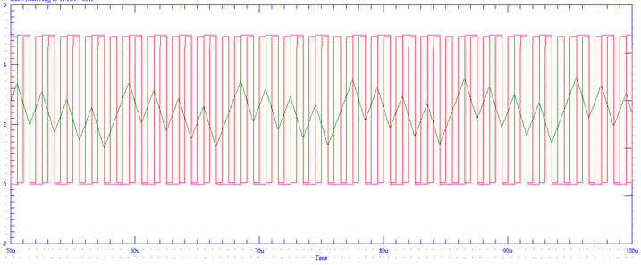
It is be noted that there is a duty
cycle within a duty cycle. That is, the single cycle duty cycle oscillates
within another approximate triangle wave duty cycle. Although the duty cycle
oscillation, in this case is approximately triangular, arguably, it may be
approximated to first order by a sine wave such that the “instantaneous” duty
cycle may be expressed as:
D
n
=(
τ
T
o
)sin(
ω
n
t)
MathType@MTEF@5@5@+=feaagCart1ev2aqatCvAUfeBSjuyZL2yd9gzLbvyNv2CaerbuLwBLnhiov2DGi1BTfMBaeXatLxBI9gBaerbd9wDYLwzYbItLDharqqtubsr4rNCHbGeaGqiVv0Je9sqqrpepC0xbbL8F4rqaqFfpeea0xe9Lq=Jc9vqaqpepm0xbba9pwe9Q8fs0=yqaqpepae9pg0FirpepeKkFr0xfr=xfr=xb9adbaqaaeGaciGaaiaabeqaamaabaabaaGcbaGaamiramaaBaaaleaacaWGUbaabeaakiabg2da9iaacIcadaWcaaqaaiabes8a0bqaaiaadsfadaWgaaWcbaGaam4BaaqabaaaaOGaaiykaiGacohacaGGPbGaaiOBaiaacIcacqaHjpWDdaWgaaWcbaGaamOBaaqabaGccaWG0bGaaiykaaaa@462E@
Where it is recognised that the sub duty
cycle variations produces a lower frequency noise ripple frequency in the
demodulated output.
Duty Cycle Noise
As noted, there is a noise error in the output
duty cycle, due to time quantisation, given by a peak step size of:
τ
np
=
1
F
s
MathType@MTEF@5@5@+=feaagCart1ev2aqatCvAUfeBSjuyZL2yd9gzLbvyNv2CaerbuLwBLnhiov2DGi1BTfMBaeXatLxBI9gBaerbd9wDYLwzYbItLDharqqtubsr4rNCHbGeaGqiVv0Je9sqqrpepC0xbbL8F4rqaqFfpeea0xe9Lq=Jc9vqaqpepm0xbba9pwe9Q8fs0=yqaqpepae9pg0FirpepeKkFr0xfr=xfr=xb9adbaqaaeGaciGaaiaabeqaamaabaabaaGcbaGaeqiXdq3aaSbaaSqaaiaad6gacaWGWbaabeaakiabg2da9maalaaabaGaaGymaaqaaiaadAeadaWgaaWcbaGaam4Caaqabaaaaaaa@3D88@
By the usual statistical arguments, it
may be stated that this time error can be expressed as a mean square error of:
σ
τn
=
1
12
F
s
MathType@MTEF@5@5@+=feaagCart1ev2aqatCvAUfeBSjuyZL2yd9gzLbvyNv2CaerbuLwBLnhiov2DGi1BTfMBaeXatLxBI9gBaerbd9wDYLwzYbItLDharqqtubsr4rNCHbGeaGqiVv0Je9sqqrpepC0xbbL8F4rqaqFfpeea0xe9Lq=Jc9vqaqpepm0xbba9pwe9Q8fs0=yqaqpepae9pg0FirpepeKkFr0xfr=xfr=xb9adbaqaaeGaciGaaiaabeqaamaabaabaaGcbaGaeq4Wdm3aaSbaaSqaaiabes8a0jaad6gaaeqaaOGaeyypa0ZaaSaaaeaacaaIXaaabaWaaOaaaeaacaaIXaGaaGOmaaWcbeaakiaadAeadaWgaaWcbaGaam4Caaqabaaaaaaa@3FF2@
The on time, which determines the
average duty cycle, and hence the average converted voltage, is obtained by
discrete additive counts of this 1/Fs step size as n/m. Assuming
that the duty cycle is changing, essentially, statistically randomly as it
hunts to the true average value, then the total error in the quantisation time
will be given by a power sum such that:
σ
τon
=
n
σ
τn
MathType@MTEF@5@5@+=feaagCart1ev2aqatCvAUfeBSjuyZL2yd9gzLbvyNv2CaerbuLwBLnhiov2DGi1BTfMBaeXatLxBI9gBaerbd9wDYLwzYbItLDharqqtubsr4rNCHbGeaGqiVv0Je9sqqrpepC0xbbL8F4rqaqFfpeea0xe9Lq=Jc9vqaqpepm0xbba9pwe9Q8fs0=yqaqpepae9pg0FirpepeKkFr0xfr=xfr=xb9adbaqaaeGaciGaaiaabeqaamaabaabaaGcbaGaeq4Wdm3aaSbaaSqaaiabes8a0jaad+gacaWGUbaabeaakiabg2da9maakaaabaGaamOBaaWcbeaakiabeo8aZnaaBaaaleaacqaHepaDcaWGUbaabeaaaaa@424F@
Where the output duty cycle,
proportional to Vin/Vref, is expressed by:
D
o
=
τ
o
T
o
=
n
τ
s
m
τ
s
MathType@MTEF@5@5@+=feaagCart1ev2aaatCvAUfeBSjuyZL2yd9gzLbvyNv2CaerbuLwBLnhiov2DGi1BTfMBaeXatLxBI9gBaerbd9wDYLwzYbItLDharqqtubsr4rNCHbGeaGqiVv0Je9sqqrpepC0xbbL8F4rqaqFfpeea0xe9Lq=Jc9vqaqpepm0xbba9pwe9Q8fs0=yqaqpepae9pg0FirpepeKkFr0xfr=xfr=xb9adbaqaaeGaciGaaiaabeqaamaabaabaaGcbaGaamiramaaBaaaleaacaWGVbaabeaakiabg2da9maalaaabaGaeqiXdq3aaSbaaSqaaiaad+gaaeqaaaGcbaGaamivamaaBaaaleaacaWGVbaabeaaaaGccqGH9aqpdaWcaaqaaiaad6gacqaHepaDdaWgaaWcbaGaam4CaaqabaaakeaacaWGTbGaeqiXdq3aaSbaaSqaaiaadohaaeqaaaaaaaa@46B6@
This results in a nominal duty cycle/voltage
quantisation “noise” error as:
D
nr
=
V
nr
=
σ
τon
/
T
o
τ
o
/
T
o
=
n
σ
τn
n
τ
s
=
1
n
12
MathType@MTEF@5@5@+=feaagCart1ev2aaatCvAUfeBSjuyZL2yd9gzLbvyNv2CaerbuLwBLnhiov2DGi1BTfMBaeXatLxBI9gBaerbd9wDYLwzYbItLDharqqtubsr4rNCHbGeaGqiVv0Je9sqqrpepC0xbbL8F4rqaqFfpeea0xe9Lq=Jc9vqaqpepm0xbba9pwe9Q8fs0=yqaqpepae9pg0FirpepeKkFr0xfr=xfr=xb9adbaqaaeGaciGaaiaabeqaamaabaabaaGcbaGaamiramaaBaaaleaacaWGUbGaamOCaaqabaGccqGH9aqpcaWGwbWaaSbaaSqaaiaad6gacaWGYbaabeaakiabg2da9maalaaabaGaeq4Wdm3aaSbaaSqaaiabes8a0jaad+gacaWGUbaabeaakiaac+cacaWGubWaaSbaaSqaaiaad+gaaeqaaaGcbaGaeqiXdq3aaSbaaSqaaiaad+gaaeqaaOGaai4laiaadsfadaWgaaWcbaGaam4BaaqabaaaaOGaeyypa0ZaaSaaaeaadaGcaaqaaiaad6gaaSqabaGccqaHdpWCdaWgaaWcbaGaeqiXdqNaamOBaaqabaaakeaacaWGUbGaeqiXdq3aaSbaaSqaaiaadohaaeqaaaaakiabg2da9maalaaabaGaaGymaaqaamaakaaabaGaamOBaaWcbeaakmaakaaabaGaaGymaiaaikdaaSqabaaaaaaa@5B24@
This expression simply represents that,
with a fixed time quantisation error, increasing the measurement time results
in that time being known relatively more accurately.
Consider the cases where m=n+1, and n
>>1, with n stepped. That is, duty cycles > 50%. This will produce a rectangular
voltage error output with a steady state duty cycle, at a frequency:
F
n
=
1
2
τ
s
(n+1)
~
F
s
2n
MathType@MTEF@5@5@+=feaagCart1ev2aaatCvAUfeBSjuyZL2yd9gzLbvyNv2CaerbuLwBLnhiov2DGi1BTfMBaeXatLxBI9gBaerbd9wDYLwzYbItLDharqqtubsr4rNCHbGeaGqiVv0Je9sqqrpepC0xbbL8F4rqaqFfpeea0xe9Lq=Jc9vqaqpepm0xbba9pwe9Q8fs0=yqaqpepae9pg0FirpepeKkFr0xfr=xfr=xb9adbaqaaeGaciGaaiaabeqaamaabaabaaGcbaGaamOramaaBaaaleaacaWGUbaabeaakiabg2da9maalaaabaGaaGymaaqaaiaaikdacqaHepaDdaWgaaWcbaGaam4CaaqabaGccaGGOaGaamOBaiabgUcaRiaaigdacaGGPaaaaiaac6hadaWcaaqaaiaadAeadaWgaaWcbaGaam4CaaqabaaakeaacaaIYaGaamOBaaaaaaa@45FB@
Therefore,
the Dnr can be expressed by substituting for n, as:
D
nr
=
1
12
.
1
F
s
2
F
n
=
D
nr
OSR
MathType@MTEF@5@5@+=feaagCart1ev2aaatCvAUfeBSjuyZL2yd9gzLbvyNv2CaerbuLwBLnhiov2DGi1BTfMBaeXatLxBI9gBaerbd9wDYLwzYbItLDharqqtubsr4rNCHbGeaGqiVv0Je9sqqrpepC0xbbL8F4rqaqFfpeea0xe9Lq=Jc9vqaqpepm0xbba9pwe9Q8fs0=yqaqpepae9pg0FirpepeKkFr0xfr=xfr=xb9adbaqaaeGaciGaaiaabeqaamaabaabaaGcbaGaamiramaaBaaaleaacaWGUbGaamOCaaqabaGccqGH9aqpdaWcaaqaaiaaigdaaeaadaGcaaqaaiaaigdacaaIYaaaleqaaaaakiaac6cadaWcaaqaaiaaigdaaeaadaGcaaqaamaalaaabaGaamOramaaBaaaleaacaWGZbaabeaaaOqaaiaaikdacaWGgbWaaSbaaSqaaiaad6gaaeqaaaaaaeqaaaaakiabg2da9maalaaabaGaamiramaaBaaaleaacaWGUbGaamOCaaqabaaakeaadaGcaaqaaiaad+eacaWGtbGaamOuaaWcbeaaaaaaaa@491D@
Where OSR is the so called Over Sampling
Ratio. This is because if the input frequency is greater than this noise
frequency, then this noise frequency cannot be filtered out. So, the input
frequency must be chosen to be less then than this noise frequency, and in the
limit, be equal to this noise frequency, so that the duty cycle noise can then be
expressed as:
D
nr
=
1
12
.
1
F
s
2
F
i
=
D
nr
OSR
MathType@MTEF@5@5@+=feaagCart1ev2aaatCvAUfeBSjuyZL2yd9gzLbvyNv2CaerbuLwBLnhiov2DGi1BTfMBaeXatLxBI9gBaerbd9wDYLwzYbItLDharqqtubsr4rNCHbGeaGqiVv0Je9sqqrpepC0xbbL8F4rqaqFfpeea0xe9Lq=Jc9vqaqpepm0xbba9pwe9Q8fs0=yqaqpepae9pg0FirpepeKkFr0xfr=xfr=xb9adbaqaaeGaciGaaiaabeqaamaabaabaaGcbaGaamiramaaBaaaleaacaWGUbGaamOCaaqabaGccqGH9aqpdaWcaaqaaiaaigdaaeaadaGcaaqaaiaaigdacaaIYaaaleqaaaaakiaac6cadaWcaaqaaiaaigdaaeaadaGcaaqaamaalaaabaGaamOramaaBaaaleaacaWGZbaabeaaaOqaaiaaikdacaWGgbWaaSbaaSqaaiaadMgaaeqaaaaaaeqaaaaakiabg2da9maalaaabaGaamiramaaBaaaleaacaWGUbGaamOCaaqabaaakeaadaGcaaqaaiaad+eacaWGtbGaamOuaaWcbeaaaaaaaa@4918@
Comparator/Sampler Linear Duty Cycle Model
Unlike in the amplitude domain, an ideal
comparator produces no error for a
τ
MathType@MTEF@5@5@+=feaagCart1ev2aqatCvAUfeBSjuyZL2yd9gzLbvyNv2CaerbuLwBLnhiov2DGi1BTfMBaeXatLxBI9gBaerbd9wDYLwzYbItLDharqqtubsr4rNCHbGeaGqiVv0Je9sqqrpepC0xbbL8F4rqaqFfpeea0xe9Lq=Jc9vqaqpepm0xbba9pwe9Q8fs0=yqaqpepae9pg0FirpepeKkFr0xfr=xfr=xb9adbaqaaeGaciGaaiaabeqaamaabaabaaGcbaGaeqiXdqhaaa@37AA@
/T input, and so a
τ
MathType@MTEF@5@5@+=feaagCart1ev2aqatCvAUfeBSjuyZL2yd9gzLbvyNv2CaerbuLwBLnhiov2DGi1BTfMBaeXatLxBI9gBaerbd9wDYLwzYbItLDharqqtubsr4rNCHbGeaGqiVv0Je9sqqrpepC0xbbL8F4rqaqFfpeea0xe9Lq=Jc9vqaqpepm0xbba9pwe9Q8fs0=yqaqpepae9pg0FirpepeKkFr0xfr=xfr=xb9adbaqaaeGaciGaaiaabeqaamaabaabaaGcbaGaeqiXdqhaaa@37AA@
/T model for the comparator and sampler may be
constructed as follows:
Fig. 9

Fig. 6

The output of the comparator is simply
the input duty cycle from the integrator added to a noise duty cycle signal due
to the error caused by the sampling quantising the time.
Integrator Linear Duty Cycle Model
Fig. 3 shows that the integrator output zero
crossings, i.e., what constitutes the integrator’s output duty cycle signal to
the comparator, are simply a delayed version of the zero crossings of its
input. Furthermore, these zero crossings are clearly independent of the
integrator gain. Changing the physical integrator gain only changes the amplitude
of the integrator triangle output, which the comparator does not care about as
it only senses zero crossings. Qualitatively, the delay of the triangle zero
crossings from its peak, dictated by its input, may be viewed as equivalent to
the delay of a sine wave peak to its zero crossings, which is 90 degrees, such
that for a duty cycle model, the integrator still behaves as an integrator
for its input output transfer function. That is, as a 1/(1- z-1)
in the Z domain, and 1/s in the Laplace domain. Indeed, the equivalence of a
demodulated output of a PWM signal, as expressed by the equivalence of:
V=(
V
p
sin(
ω
i
t))
τ
Τ
MathType@MTEF@5@5@+=feaagCart1ev2aqatCvAUfeBSjuyZL2yd9gzLbvyNv2CaerbuLwBLnhiov2DGi1BTfMBaeXatLxBI9gBaerbd9wDYLwzYbItLDharqqtubsr4rNCHbGeaGqiVv0Je9sqqrpepC0xbbL8F4rqaqFfpeea0xe9Lq=Jc9vqaqpepm0xbba9pwe9Q8fs0=yqaqpepae9pg0FirpepeKkFr0xfr=xfr=xb9adbaqaaeGaciGaaiaabeqaamaabaabaaGcbaGaamOvaiabg2da9iaacIcacaWGwbWaaSbaaSqaaiaadchaaeqaaOGaci4CaiaacMgacaGGUbGaaiikaiabeM8a3naaBaaaleaacaWGPbaabeaakiaadshacaGGPaGaaiykamaalaaabaGaeqiXdqhabaGaeuiPdqfaaaaa@469B@
V=
V
p
(
τ
Τ
sin(
ω
i
t))
MathType@MTEF@5@5@+=feaagCart1ev2aqatCvAUfeBSjuyZL2yd9gzLbvyNv2CaerbuLwBLnhiov2DGi1BTfMBaeXatLxBI9gBaerbd9wDYLwzYbItLDharqqtubsr4rNCHbGeaGqiVv0Je9sqqrpepC0xbbL8F4rqaqFfpeea0xe9Lq=Jc9vqaqpepm0xbba9pwe9Q8fs0=yqaqpepae9pg0FirpepeKkFr0xfr=xfr=xb9adbaqaaeGaciGaaiaabeqaamaabaabaaGcbaGaamOvaiabg2da9iaadAfadaWgaaWcbaGaamiCaaqabaGccaGGOaWaaSaaaeaacqaHepaDaeaacqqHKoavaaGaci4CaiaacMgacaGGUbGaaiikaiabeM8a3naaBaaaleaacaWGPbaabeaakiaadshacaGGPaGaaiykaaaa@469B@
Shows that any filter will process a PWM
signal in essentially the same manner as that of an amplitude signal.
It is noted that in general, the zero
crossings of the output of an integrator, do not usually remain the same as
that of it input. For an open loop integrator, any average DC due to unequal
duty cycle will result in an ever increasing amplitude output.
However, for the integrator, it still remains
to determine its gain constant for an applied duty cycle transfer function.
As the output duty cycle of the integrator is the same as its input duty cycle,
the small signal transfer gain of the integrator model for a sinusoidal duty
cycle variation must then also be unity.
Consider the following block continuous
time model:
Fig.
7

An analysis of the above model, and confirmation
simulations, shows that K must be 1 if the modulation frequency is to result in
equal amplitude demodulated PWM outputs at that frequency. That is, equal
effective PWM signals prior to the LPF, irrespective of the triangle and
rectangular input waveform shapes to the LPFs. The duty cycle is changed at the
rate of the sample frequency Fs, hence the constant K, should be set to 1 at
Fs, which sets K to unity for the Z domain integrator.
Thus, the duty cycle, Z domain linear model for the
Delta-Sigma converter is:
Fig. 10
Aylward Duty
Cycle Model

Where it may be noted that there is now no room to
move the comparator gain into the integrator gain as the comparator has been necessarily
modelled by a unity gain duty cycle transfer function, not as an amplifier.
Time Domain View of Noise Shaping
A higher frequency, variable duty cycle is produced
so that the average of the duty cycle still produces the same average of the
input voltage ratio.
A search on the internet, despite there being many
tutorials on Delta-Sigma converters, essentially, turns up nothing for any time
domain explanations of so called “noise shaping”. Typically there is an
overview and then a jaunt into the small signal (flawed) model, essentially,
allegedly claiming that the amplitude “noise” of the comparator gets filtered
in such a way as to “push low frequency noise up in frequency”. What is really
happening?
For voltages near full scale or zero, and with 1/N
ratio, it is has been illustrated that a constant
τ
MathType@MTEF@5@5@+=feaagCart1ev2aqatCvAUfeBSjuyZL2yd9gzLbvyNv2CaerbuLwBLnhiov2DGi1BTfMBaeXatLxBI9gBaerbd9wDYLwzYbItLDharqqtubsr4rNCHbGeaGqiVv0Je9sqqrpepC0xbbL8F4rqaqFfpeea0xe9Lq=Jc9vqaqpepm0xbba9pwe9Q8fs0=yqaqpepae9pg0FirpepeKkFr0xfr=xfr=xb9adbaqaaeGaciGaaiaabeqaamaabaabaaGcbaGaeqiXdqhaaa@37AA@
/T digital output at a sample frequency/N is
produced. For ratios where there is room for higher and lower
τ
MathType@MTEF@5@5@+=feaagCart1ev2aqatCvAUfeBSjuyZL2yd9gzLbvyNv2CaerbuLwBLnhiov2DGi1BTfMBaeXatLxBI9gBaerbd9wDYLwzYbItLDharqqtubsr4rNCHbGeaGqiVv0Je9sqqrpepC0xbbL8F4rqaqFfpeea0xe9Lq=Jc9vqaqpepm0xbba9pwe9Q8fs0=yqaqpepae9pg0FirpepeKkFr0xfr=xfr=xb9adbaqaaeGaciGaaiaabeqaamaabaabaaGcbaGaeqiXdqhaaa@37AA@
/T lower ratios, things are different.
Consider a 269/1024 ratio, chosen specifically as a prime number numerator so
that there is only one exact solution to the average voltage that that ratio
represents, i.e. 0.26269. Simulations show that this does not produce an exact
269 count/1024 count at a 1024 times sample period, but what initially appears
to be a 1 count/5 count, representing 0.2 at a much higher frequency, but still
with the correct average output voltage! Further examination of the
waveforms show that, spread through time, the counts change.
Thus the Sigma Delta converter, changes
what would otherwise be a full scale amplitude duty cycle at a low frequency,
to a variable duty cycle at a much higher frequency that still averages to the
same value. This higher frequency variable duty cycle might well have a lower frequency
component due to the repetitive count modifications, at the frequency that
would be expected for an exact count, but this component is much reduced in
spectral amplitude. It is only a modulation, not a fundamental frequency.
A more detailed account of exactly what "noise
shaping" is, is described in Noise Shaping As Error Correction.
Summary
It has been shown that the standard amplitude based
linear model of Delta-Sigma converters is trivially invalid, and that a model
based on duty cycle is mathematically consistent and correctly accounts for
characteristics amenable to linear analysis where the standard model fails.
Indeed, the standard linear model’s alleged account of noise filtering is
entirely delusionary and essentially, explains nothing. The non linear
comparator ensures that an amplitude based transfer function argument is DOA.
The Delta-Sigma converter is now seen to be based
on an average duty cycle linear transfer function such that feedback is then
able to correct for duty cycle errors. It is the large duty cycle gain at low
frequencies that allows for the errors to be reduced, not amplitude gain. A
Delta Sigma converter, essentially, operates in the time domain, not amplitude
domain.
References
1 - “Understanding Sigma-Delta Modulation: The
Solved and Unresolved Issues”
–
MathType@MTEF@5@5@+=feaagCart1ev2aqatCvAUfeBSjuyZL2yd9gzLbvyNv2CaerbuLwBLnhiov2DGi1BTfMBaeXatLxBI9gBaerbd9wDYLwzYbItLDharqqtubsr4rNCHbGeaGqiVu0Je9sqqrpepC0xbbL8F4rqqrFfpeea0xe9Lq=Jc9vqaqpepm0xbba9pwe9Q8fs0=yqaqpepae9pg0FirpepeKkFr0xfr=xfr=xb9adbaqaaeGaciGaaiaabeqaamaabaabaaGcbaacbaqcLbyaqaaaaaaaaaWdbiaa=nbiaaa@37C1@
Joshua D. Reiss, J. Audio Eng. Soc Vol 56 no.
½
MathType@MTEF@5@5@+=feaagCart1ev2aqatCvAUfeBSjuyZL2yd9gzLbvyNv2CaerbuLwBLnhiov2DGi1BTfMBaeXatLxBI9gBaerbd9wDYLwzYbItLDharqqtubsr4rNCHbGeaGqiVu0Je9sqqrpepC0xbbL8F4rqqrFfpeea0xe9Lq=Jc9vqaqpepm0xbba9pwe9Q8fs0=yqaqpepae9pg0FirpepeKkFr0xfr=xfr=xb9adbaqaaeGaciGaaiaabeqaamaabaabaaGcbaacbaqcLbyaqaaaaaaaaaWdbiaa=1laaaa@384B@
, 2008 January/February
2
–
MathType@MTEF@5@5@+=feaagCart1ev2aqatCvAUfeBSjuyZL2yd9gzLbvyNv2CaerbuLwBLnhiov2DGi1BTfMBaeXatLxBI9gBaerbd9wDYLwzYbItLDharqqtubsr4rNCHbGeaGqiVu0Je9sqqrpepC0xbbL8F4rqqrFfpeea0xe9Lq=Jc9vqaqpepm0xbba9pwe9Q8fs0=yqaqpepae9pg0FirpepeKkFr0xfr=xfr=xb9adbaqaaeGaciGaaiaabeqaamaabaabaaGcbaacbaqcLbyaqaaaaaaaaaWdbiaa=nbiaaa@37C1@
“An Overview of Sigma-Delta Converters: How a
1-Bit ADC achieves more than 16 bit Resolution”
–
MathType@MTEF@5@5@+=feaagCart1ev2aqatCvAUfeBSjuyZL2yd9gzLbvyNv2CaerbuLwBLnhiov2DGi1BTfMBaeXatLxBI9gBaerbd9wDYLwzYbItLDharqqtubsr4rNCHbGeaGqiVu0Je9sqqrpepC0xbbL8F4rqqrFfpeea0xe9Lq=Jc9vqaqpepm0xbba9pwe9Q8fs0=yqaqpepae9pg0FirpepeKkFr0xfr=xfr=xb9adbaqaaeGaciGaaiaabeqaamaabaabaaGcbaacbaqcLbyaqaaaaaaaaaWdbiaa=nbiaaa@37C1@
Pervez M. Aziz, Bell Laboratories, Henrik V.
Sorensen, Arial Corporation, Jan Van der Spiegel, University of Pennsylvania
3
–
MathType@MTEF@5@5@+=feaagCart1ev2aqatCvAUfeBSjuyZL2yd9gzLbvyNv2CaerbuLwBLnhiov2DGi1BTfMBaeXatLxBI9gBaerbd9wDYLwzYbItLDharqqtubsr4rNCHbGeaGqiVu0Je9sqqrpepC0xbbL8F4rqqrFfpeea0xe9Lq=Jc9vqaqpepm0xbba9pwe9Q8fs0=yqaqpepae9pg0FirpepeKkFr0xfr=xfr=xb9adbaqaaeGaciGaaiaabeqaamaabaabaaGcbaacbaqcLbyaqaaaaaaaaaWdbiaa=nbiaaa@37C1@
“Delta-Sigma Data Converters, Theory, Design
and Simulation” - Norsworthy et al (1997), p143
4 - "Idle tone behaviour in Sigma Delta
Modulation" - Enrique Perez Gonzalez1, and Joshua Reiss1, Audio
Engineering Society 122nd Convention 2007 May 5
–
MathType@MTEF@5@5@+=feaagCart1ev2aqatCvAUfeBSjuyZL2yd9gzLbvyNv2CaerbuLwBLnhiov2DGi1BTfMBaeXatLxBI9gBaerbd9wDYLwzYbItLDharqqtubsr4rNCHbGeaGqiVu0Je9sqqrpepC0xbbL8F4rqqrFfpeea0xe9Lq=Jc9vqaqpepm0xbba9pwe9Q8fs0=yqaqpepae9pg0FirpepeKkFr0xfr=xfr=xb9adbaqaaeGaciGaaiaabeqaamaabaabaaGcbaacbaqcLbyaqaaaaaaaaaWdbiaa=nbiaaa@37C1@
8 Vienna, Austria
5
–
MathType@MTEF@5@5@+=feaagCart1ev2aqatCvAUfeBSjuyZL2yd9gzLbvyNv2CaerbuLwBLnhiov2DGi1BTfMBaeXatLxBI9gBaerbd9wDYLwzYbItLDharqqtubsr4rNCHbGeaGqiVu0Je9sqqrpepC0xbbL8F4rqqrFfpeea0xe9Lq=Jc9vqaqpepm0xbba9pwe9Q8fs0=yqaqpepae9pg0FirpepeKkFr0xfr=xfr=xb9adbaqaaeGaciGaaiaabeqaamaabaabaaGcbaacbaqcLbyaqaaaaaaaaaWdbiaa=nbiaaa@37C1@
“Sigma-Delta Modulators: Tutorial Overview,
Design Guide, and State-of-the-Art Survey Circuits and Systems I:” Regular
Papers, IEEE Transactions on (Volume:58
, Issue: 1 ) Pub. Dec. 2010
6
–
MathType@MTEF@5@5@+=feaagCart1ev2aqatCvAUfeBSjuyZL2yd9gzLbvyNv2CaerbuLwBLnhiov2DGi1BTfMBaeXatLxBI9gBaerbd9wDYLwzYbItLDharqqtubsr4rNCHbGeaGqiVu0Je9sqqrpepC0xbbL8F4rqqrFfpeea0xe9Lq=Jc9vqaqpepm0xbba9pwe9Q8fs0=yqaqpepae9pg0FirpepeKkFr0xfr=xfr=xb9adbaqaaeGaciGaaiaabeqaamaabaabaaGcbaacbaqcLbyaqaaaaaaaaaWdbiaa=nbiaaa@37C1@
“ADC Architectures III: Sigma-Delta ADC Basics”
- Walt Kester
–
MathType@MTEF@5@5@+=feaagCart1ev2aqatCvAUfeBSjuyZL2yd9gzLbvyNv2CaerbuLwBLnhiov2DGi1BTfMBaeXatLxBI9gBaerbd9wDYLwzYbItLDharqqtubsr4rNCHbGeaGqiVu0Je9sqqrpepC0xbbL8F4rqqrFfpeea0xe9Lq=Jc9vqaqpepm0xbba9pwe9Q8fs0=yqaqpepae9pg0FirpepeKkFr0xfr=xfr=xb9adbaqaaeGaciGaaiaabeqaamaabaabaaGcbaacbaqcLbyaqaaaaaaaaaWdbiaa=nbiaaa@37C1@
Analog Devise App note MT-022
7
–
MathType@MTEF@5@5@+=feaagCart1ev2aqatCvAUfeBSjuyZL2yd9gzLbvyNv2CaerbuLwBLnhiov2DGi1BTfMBaeXatLxBI9gBaerbd9wDYLwzYbItLDharqqtubsr4rNCHbGeaGqiVu0Je9sqqrpepC0xbbL8F4rqqrFfpeea0xe9Lq=Jc9vqaqpepm0xbba9pwe9Q8fs0=yqaqpepae9pg0FirpepeKkFr0xfr=xfr=xb9adbaqaaeGaciGaaiaabeqaamaabaabaaGcbaacbaqcLbyaqaaaaaaaaaWdbiaa=nbiaaa@37C1@
“ADC Architectures IV: Sigma-Delta ADC
Advanced Concepts and Applications" - Walt Kester - Analog Devices App
note MT-023
8
–
MathType@MTEF@5@5@+=feaagCart1ev2aqatCvAUfeBSjuyZL2yd9gzLbvyNv2CaerbuLwBLnhiov2DGi1BTfMBaeXatLxBI9gBaerbd9wDYLwzYbItLDharqqtubsr4rNCHbGeaGqiVu0Je9sqqrpepC0xbbL8F4rqqrFfpeea0xe9Lq=Jc9vqaqpepm0xbba9pwe9Q8fs0=yqaqpepae9pg0FirpepeKkFr0xfr=xfr=xb9adbaqaaeGaciGaaiaabeqaamaabaabaaGcbaacbaqcLbyaqaaaaaaaaaWdbiaa=nbiaaa@37C1@
“Demystifying Delta-Sigma ADCs” Tutorial 1870
- App Note
–
MathType@MTEF@5@5@+=feaagCart1ev2aqatCvAUfeBSjuyZL2yd9gzLbvyNv2CaerbuLwBLnhiov2DGi1BTfMBaeXatLxBI9gBaerbd9wDYLwzYbItLDharqqtubsr4rNCHbGeaGqiVu0Je9sqqrpepC0xbbL8F4rqqrFfpeea0xe9Lq=Jc9vqaqpepm0xbba9pwe9Q8fs0=yqaqpepae9pg0FirpepeKkFr0xfr=xfr=xb9adbaqaaeGaciGaaiaabeqaamaabaabaaGcbaacbaqcLbyaqaaaaaaaaaWdbiaa=nbiaaa@37C1@
Jan 31, 2003 - Maxim Integrated
9
–
MathType@MTEF@5@5@+=feaagCart1ev2aqatCvAUfeBSjuyZL2yd9gzLbvyNv2CaerbuLwBLnhiov2DGi1BTfMBaeXatLxBI9gBaerbd9wDYLwzYbItLDharqqtubsr4rNCHbGeaGqiVu0Je9sqqrpepC0xbbL8F4rqqrFfpeea0xe9Lq=Jc9vqaqpepm0xbba9pwe9Q8fs0=yqaqpepae9pg0FirpepeKkFr0xfr=xfr=xb9adbaqaaeGaciGaaiaabeqaamaabaabaaGcbaacbaqcLbyaqaaaaaaaaaWdbiaa=nbiaaa@37C1@
“How delta-sigma ADCs work, Part 1” - Bonnie
Baker - App Note - Texas Instruments
10
–
MathType@MTEF@5@5@+=feaagCart1ev2aqatCvAUfeBSjuyZL2yd9gzLbvyNv2CaerbuLwBLnhiov2DGi1BTfMBaeXatLxBI9gBaerbd9wDYLwzYbItLDharqqtubsr4rNCHbGeaGqiVu0Je9sqqrpepC0xbbL8F4rqqrFfpeea0xe9Lq=Jc9vqaqpepm0xbba9pwe9Q8fs0=yqaqpepae9pg0FirpepeKkFr0xfr=xfr=xb9adbaqaaeGaciGaaiaabeqaamaabaabaaGcbaacbaqcLbyaqaaaaaaaaaWdbiaa=nbiaaa@37C1@
“Principals of Sigma Delta Modulation for
Analog to Digital Converters” - Sangil Park, Ph. D.
–
MathType@MTEF@5@5@+=feaagCart1ev2aqatCvAUfeBSjuyZL2yd9gzLbvyNv2CaerbuLwBLnhiov2DGi1BTfMBaeXatLxBI9gBaerbd9wDYLwzYbItLDharqqtubsr4rNCHbGeaGqiVu0Je9sqqrpepC0xbbL8F4rqqrFfpeea0xe9Lq=Jc9vqaqpepm0xbba9pwe9Q8fs0=yqaqpepae9pg0FirpepeKkFr0xfr=xfr=xb9adbaqaaeGaciGaaiaabeqaamaabaabaaGcbaacbaqcLbyaqaaaaaaaaaWdbiaa=nbiaaa@37C1@
Motorola
11 "Delta Sigma AD Conversion
Technique Overview" - AN10 -Crystal Semiconductor, A Cirrus Logic Company.
“…The
quantization noise at the output is reduced by the open-loop gain of the
integrator. At low frequency, the integrator is designed for high open-loop
gain, so that quantization noise is reduced...”
12 "Why 1-Bit Sigma-Delta Conversion
is Unsuitable for High-Quality Applications" - Stanley P. Lipshitz and
John Vanderkooy Audio Research Group, University of Waterloo
Waterloo, Ontario N2L 3G1, Canada -
Audio Engineering Society Convention Paper 5395 Presented at the 110th
Convention 2001 May 12
–
MathType@MTEF@5@5@+=feaagCart1ev2aqatCvAUfeBSjuyZL2yd9gzLbvyNv2CaerbuLwBLnhiov2DGi1BTfMBaeXatLxBI9gBaerbd9wDYLwzYbItLDharqqtubsr4rNCHbGeaGqiVu0Je9sqqrpepC0xbbL8F4rqqrFfpeea0xe9Lq=Jc9vqaqpepm0xbba9pwe9Q8fs0=yqaqpepae9pg0FirpepeKkFr0xfr=xfr=xb9adbaqaaeGaciGaaiaabeqaamaabaabaaGcbaacbaqcLbyaqaaaaaaaaaWdbiaa=nbiaaa@37C1@
15 Amsterdam,
The Netherlands
23 - Noise Shaping As Error Correction
© Kevin
Aylward 2013
All
rights reserved
The
information on the page may be reproduced
providing
that this source is acknowledged.
Website
last modified 30th August 2013
www.kevinaylward.co.uk